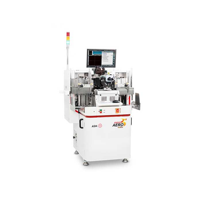
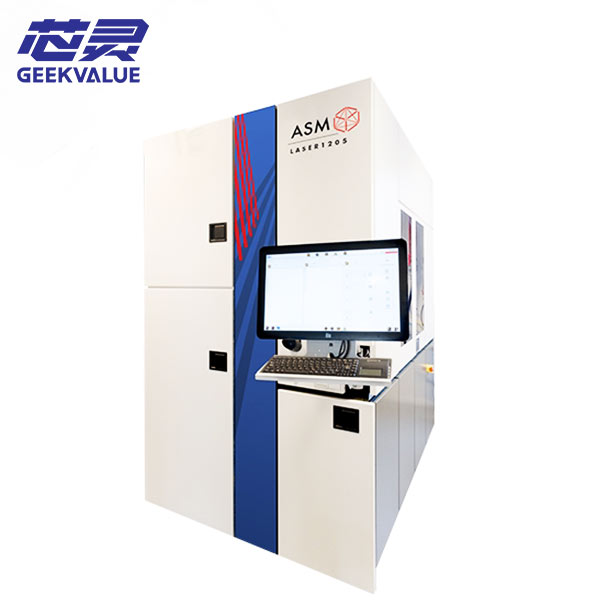
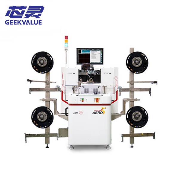
The ASM AD838, developed by ASMPT, is a high-volume production die attach platform designed for mature semiconductor packaging applications. It is widely used in LED assembly, discrete semiconductor packaging, and standard IC manufacturing where process stability and throughput efficiency are primary requirements.
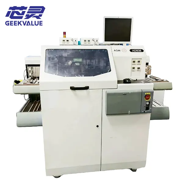
Overview of ASM AD838 Die Bonding System
The ASM AD838 is a fully automated epoxy die bonding machine optimized for high-throughput backend semiconductor manufacturing. It is designed for stable long-cycle production environments, providing consistent die placement accuracy, robust mechanical operation, and low process variability.
This system is commonly deployed in OSAT and IDM production lines focusing on LED devices, power discretes, and mainstream integrated circuits where ultra-fine-pitch advanced packaging is not required.
What is ASM AD838 Used For?
The AD838 is used for high-speed epoxy die attach processes in semiconductor packaging. It picks silicon dies, LED chips, or discrete components and places them onto leadframes or organic substrates using controlled adhesive dispensing and vision-guided alignment.
The platform is optimized for mass production environments requiring stable throughput, predictable maintenance cycles, and consistent bond quality across long production runs.
Key Industry Applications
LED & Optoelectronics Packaging
High-brightness LED chip assembly (HB-LED)
Backlighting modules for displays
Photodiodes and basic optical sensors
Power Semiconductor Devices
Power MOSFETs and bipolar transistors
Rectifier diodes and discrete power components
Standard power management IC packaging
Consumer & Industrial Electronics
Microcontrollers and logic ICs
Standard digital and analog semiconductor devices
Cost-sensitive high-volume consumer electronics
Competitive Positioning in Die Bonding Equipment
The ASM AD838 is positioned as a high-throughput, cost-efficient die bonding platform for mature semiconductor production lines. It prioritizes mechanical reliability and production stability over advanced packaging capabilities such as flip chip or eutectic bonding.
Compared to advanced flip chip systems: Focused on epoxy die attach, not sub-micron interconnect or fine-pitch bonding.
Compared to newer high-end platforms: Offers lower CAPEX and simplified process control for mature product manufacturing.
Compared to legacy systems: Improved motion control, better vision alignment stability, and higher UPH consistency.
Technical Capability Overview
High-Throughput Epoxy Bonding: Optimized dispensing and placement system for stable mass production.
Vision Alignment System: Ensures repeatable die placement accuracy for mainstream packaging requirements.
Leadframe Handling Platform: Designed for strip-based semiconductor assembly with stable mechanical transport.
Process Stability Design: Engineered for long production cycles with minimal drift and predictable maintenance intervals.
Technical Specifications (Typical Configuration)
Specifications vary depending on die size, epoxy material, and substrate type.
| Parameter | Specification |
|---|---|
| System Type | Fully automatic epoxy die bonder |
| Placement Accuracy | ±15 μm to ±25 μm @ 3σ (process dependent) |
| Bonding Method | Epoxy dispensing / stamping die attach |
| Supported Packages | Leadframe, organic substrate, strip carriers |
| Wafer Compatibility | Up to 8-inch / 12-inch (configuration dependent) |
| Throughput | Optimized for high-volume production (UPH-focused design) |
Why Manufacturers Use ASM AD838
Reduces total cost of ownership for mature semiconductor product lines
Ensures stable long-term production with low process variation
Minimizes operator dependency through standardized process recipes
Delivers consistent yield for LED and discrete device manufacturing
Typical Semiconductor Backend Process Flow
Wafer dicing → Die attach (ASM AD838) → Wire bonding → Encapsulation (molding) → Singulation → Final electrical test
Frequently Asked Questions
What is ASM AD838 used for?
It is used for high-volume epoxy die attach in semiconductor backend manufacturing, especially for LED, discrete power devices, and standard IC packaging.
Is ASM AD838 suitable for advanced packaging?
No. The system is designed for mainstream epoxy die attach applications and does not support advanced flip chip or eutectic bonding processes.
Why do manufacturers choose AD838 over newer systems?
Because it offers a lower capital investment, stable production performance, and well-established process maturity for high-volume manufacturing lines.
Summary
The ASM AD838 die bonding system is a proven high-volume production platform for mainstream semiconductor packaging. Its strength lies in process stability, mechanical robustness, and cost efficiency, making it a reliable solution for LED, discrete, and standard IC manufacturing environments.
Request Technical Specification or Quotation
Machine specification sheet
Process integration support
Refurbished equipment availability
Production line optimization consulting
Contact / Inquiry Section