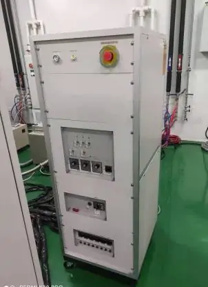
The Hitachi S-8840 is a critical-dimension scanning electron microscope developed for automated linewidth and feature-size measurement in semiconductor wafer processing. It combines low-voltage SEM imaging, wafer handling, alignment and measurement software in a production metrology platform.
The available equipment information identifies the S-8840 for 150 mm and 200 mm wafers. Published measurement performance includes a CD range of 0.1 to 10 µm and repeatability of 3σ ≤5 nm or ≤±1%, depending on the measured structure and operating conditions.
Hitachi S-8840 Main Specifications
| Manufacturer | Hitachi |
|---|---|
| Model | S-8840 |
| Equipment Type | Critical-Dimension Scanning Electron Microscope |
| Supported Wafer Sizes | 150 mm and 200 mm |
| Compatible Wafer Thickness | Approximately 0.4–1.0 mm, according to the available listing |
| Wafer Cassette Capacity | 25 wafers per cassette |
| Published Image Resolution | 5 nm |
| CD Measurement Range | 0.1–10 µm |
| CD Repeatability | 3σ ≤5 nm or ≤±1% |
| SEM Magnification | 1,000× to 150,000× |
| Optical Microscope Magnification | Approximately 110× |
| Wafer Handling | Cassette-to-cassette automatic wafer transfer and alignment |
| Condition | Used semiconductor equipment |
| Availability | Subject to current stock, inspection and configuration confirmation |
Key Equipment Features
Automated critical-dimension and linewidth measurement
Compatible with listed 150 mm and 200 mm wafer formats
Cassette-to-cassette automatic wafer handling
Automatic wafer alignment and X-Y stage positioning
Low-voltage SEM imaging for semiconductor structures
Integrated measurement, wafer-map and process-control software
Typical Applications
The Hitachi S-8840 may be used to measure photoresist lines, etched features, contact holes and other semiconductor structures requiring repeatable critical-dimension control.
Typical process-control positions may include after-development inspection, after-etch inspection and engineering analysis. Actual measurement performance depends on the feature material, charging behavior, edge contrast, recipe and calibration condition.
Used Equipment Configuration and Inspection
Before quotation, customers should confirm whether the machine is configured for 150 mm, 200 mm or both wafer formats. Cassette stations, wafer robot parts, chuck, alignment hardware and measurement recipes may differ between systems.
Important inspection points include the electron gun, electron column, apertures, detectors, vacuum system, wafer handler, X-Y stage, control computer, software license, calibration standards and current measurement repeatability.
Request Hitachi S-8840 Information
Contact our team to check the current availability of the used Hitachi S-8840. Please provide your wafer size, feature type, expected CD range, process-control application, destination country and installation schedule.
Contact us for equipment photos, wafer-handling configuration, inspection results and quotation.
Frequently Asked Questions
What does the Hitachi S-8840 measure?
The S-8840 measures semiconductor critical dimensions such as line width, spacing and feature size using scanning electron microscope images and automated measurement software.
What wafer sizes does the S-8840 support?
The available information lists compatibility with 150 mm and 200 mm wafers. The installed loader, cassette and chuck configuration should be confirmed.
What is the listed CD measurement range?
The published range is 0.1 to 10 µm. Suitability for a specific structure depends on image contrast, feature shape, material and the measurement recipe.
What should be tested before purchasing a used CD-SEM?
Recommended checks include vacuum performance, electron-beam stability, image resolution, wafer transfer, stage accuracy, autofocus, calibration and CD repeatability using a suitable reference sample.