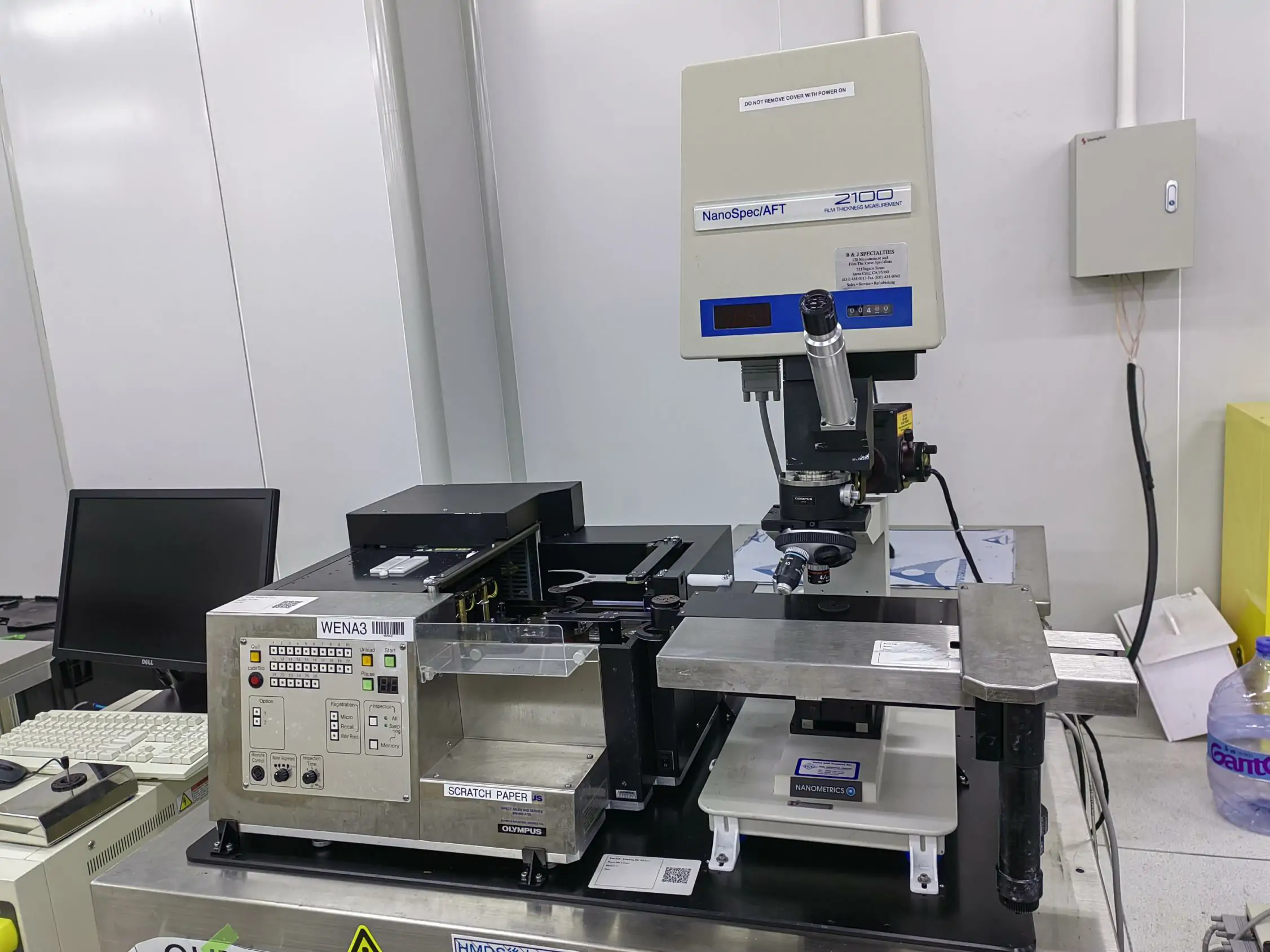
The Nanometrics NanoSpec AFT 2100 is a computerized, non-contact optical system for measuring the thickness of transparent semiconductor films. It measures reflected-light intensity across a wavelength range and calculates film thickness from optical interference.
The available equipment listing identifies this AFT 2100 for 150 mm wafers. Typical measurable materials include silicon oxide, silicon nitride, photoresist, polyimide and polysilicon-on-oxide when the optical properties and refractive index are known.
Nanometrics AFT 2100 Main Specifications
| Manufacturer | Nanometrics |
|---|---|
| Product Family | NanoSpec |
| Model | AFT 2100 |
| Equipment Type | Optical Thin-Film Thickness Measurement System |
| Listed Wafer Size | 150 mm / 6-inch |
| Measurement Method | Non-contact spectral reflectance and optical interference |
| Published Wavelength Range | 360–760 nm |
| Published Thickness Range | Less than 100 Å to approximately 50,000 Å |
| Published Reproducibility | Approximately ±2% to ±5%, depending on film and measurement conditions |
| Objective Lenses | 5×, 10× and 50× |
| Published Measurement Spot Sizes | Approximately 50 µm, 25 µm and 5 µm, depending on objective lens |
| Film Requirement | Film should be transparent within the measurement range and have known optical properties |
| Condition | Used semiconductor equipment |
| Availability | Subject to current stock, inspection and configuration confirmation |
Key Equipment Features
Non-contact optical film-thickness measurement
Computer-controlled monochromator and optical detector
Multiple objective lenses for different measurement spot sizes
Predefined programs for common semiconductor films
Suitable for dielectric, resist and compatible polysilicon film measurements
Useful for engineering, laboratory and process-monitoring applications
Typical Applications
The AFT 2100 may be used to measure silicon oxide, silicon nitride, positive or negative photoresist, polyimide and polysilicon-on-oxide films. It can support process checks after oxidation, deposition, coating or other thin-film formation steps.
The instrument is not suitable for every opaque or strongly absorbing film. Measurement accuracy depends on the film stack, refractive index, substrate, surface condition, selected optical model and calibration reference.
Used Equipment Configuration and Inspection
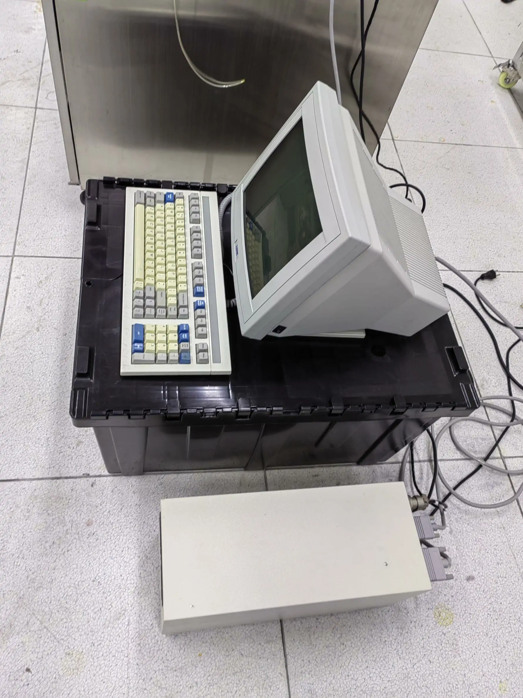
The available system should be checked for its microscope, monochromator, detector, illumination source, objective lenses, sample stage, computer, measurement software and calibration standards.
Before quotation, customers should confirm the serial number, installed objectives, supported wafer holder, lamp condition, wavelength calibration, repeatability test, available film programs and current computer operation.
Request Nanometrics AFT 2100 Information
Contact our team to check the current availability of the used Nanometrics AFT 2100. Please provide your wafer size, film material, approximate thickness range, substrate and required measurement spot size.
Contact us for equipment photos, installed objectives, measurement test results and quotation.
Frequently Asked Questions
What does the NanoSpec AFT 2100 measure?
It measures the thickness of suitable transparent thin films by analyzing reflected light and optical interference across a wavelength range.
What film materials can be measured?
Common applications include silicon oxide, silicon nitride, photoresist, polyimide and polysilicon-on-oxide. The film must have suitable optical properties and a usable measurement model.
Can the AFT 2100 measure metal films?
It is primarily intended for transparent or partially transparent films. Many opaque metal films cannot be measured with the same spectral-reflectance method.
What should be checked on a used AFT 2100?
Important checks include the light source, monochromator, detector, objective lenses, sample stage, calibration, software and repeatability on a reference wafer.