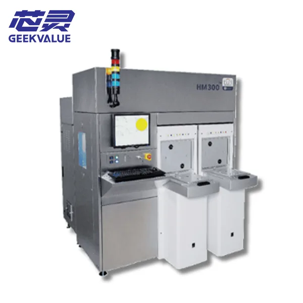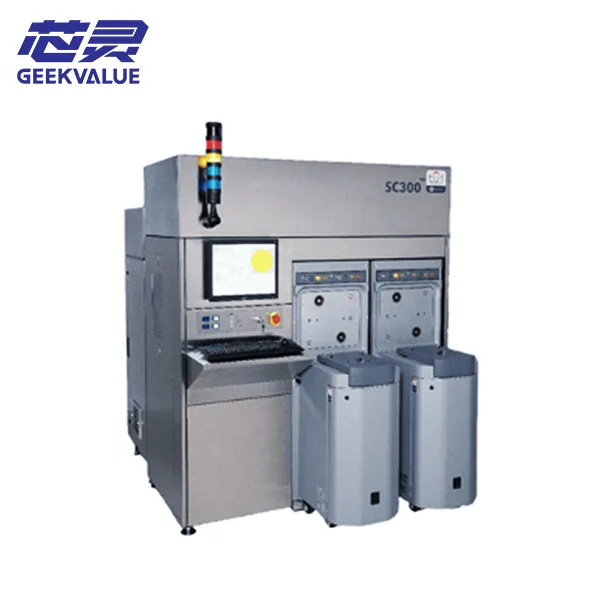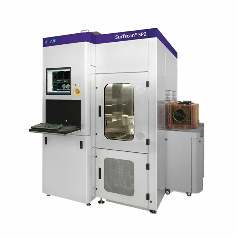
The KLA Surfscan SP2 is an unpatterned wafer inspection system designed to detect particles, scratches, surface abnormalities and other defects on semiconductor wafers. It uses ultraviolet laser illumination, dark-field optical detection and automated defect analysis.
The platform supports 200 mm and 300 mm wafers and may be used for inspecting bare silicon, smooth and rough films, photoresist layers and other compatible wafer surfaces. Actual sensitivity and throughput depend on the selected inspection mode, wafer material and condition of the available system.
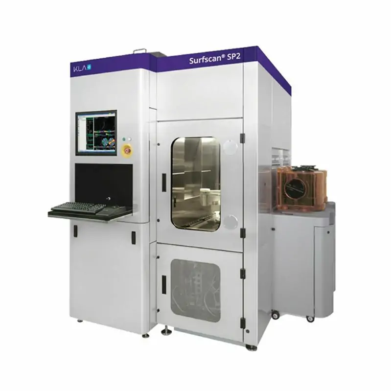
KLA Surfscan SP2 Main Specifications
| Manufacturer | KLA-Tencor / KLA |
|---|---|
| Model | Surfscan SP2 |
| Equipment Type | Unpatterned Wafer Defect Inspection System |
| Supported Wafer Sizes | 200 mm and 300 mm |
| Inspection Technology | UV laser dark-field optical inspection |
| Published Sensitivity | Defects as small as approximately 37 nm under specified wafer and inspection conditions |
| Illumination Modes | Normal-incidence and oblique-incidence illumination |
| Inspectable Surfaces | Bare wafers, smooth and rough films, film stacks and photoresist layers |
| Data Capability | Defect mapping, classification and SURFimage surface-analysis data |
| Condition | Used semiconductor equipment |
| Availability | Subject to current stock, inspection and configuration confirmation |
Key Equipment Features
UV laser-based dark-field wafer inspection
Supports 200 mm and 300 mm wafer formats
Normal and oblique optical illumination modes
Multiple sensitivity and throughput operating modes
Detection of particles, scratches and surface abnormalities
Whole-wafer defect mapping and surface-analysis capability
Typical Applications
The Surfscan SP2 can be used for incoming wafer inspection, substrate qualification, process-tool monitoring and surface-quality control. Typical inspection points may follow cleaning, deposition, polishing, epitaxy or photoresist processing.
The system may be considered for silicon, SOI and compatible compound-semiconductor substrates, including suitable SiC and GaN wafers. The inspection recipe and verified sensitivity must be matched to the wafer material and surface condition.
Used Equipment Configuration and Inspection
The available configuration should be checked for wafer size, load ports, wafer-handling hardware, laser condition, optical detectors, computer system, software version and installed analysis options.
Before quotation, customers should confirm the serial number, SP2 variant, wafer formats, system calibration, defect-detection test, robot operation, reference wafers, available documentation and current power-on status.
Request KLA Surfscan SP2 Information
Contact our team to check the current availability of the used KLA Surfscan SP2. Please provide your wafer size, wafer material, target defect size, inspection application, destination country and installation schedule.
Contact us for current equipment photos, configuration details, inspection results and quotation.
Frequently Asked Questions
Is the Surfscan SP2 used for patterned or unpatterned wafers?
The Surfscan SP2 is primarily designed for unpatterned wafer and surface inspection. Patterned-wafer defect inspection normally requires a different inspection platform.
What wafer sizes can the Surfscan SP2 inspect?
The published platform supports 200 mm and 300 mm wafers. The installed load ports and wafer-handling configuration should be confirmed on the available system.
Can the Surfscan SP2 inspect SiC and GaN wafers?
The platform has applications involving compatible SiC, GaN and other substrate materials, but sensitivity depends on surface roughness, reflectivity and the qualified inspection recipe.
Does every SP2 achieve the same 37 nm sensitivity?
No. Published sensitivity depends on the operating mode, wafer material, surface condition, calibration and installed system configuration. A sample-wafer test is recommended when sensitivity is critical.